| The
cameras and recording media available for modern digital image
processing applications are changing at a significant pace. To dwell too
long in this section on one major type of camera, such as the CCD
camera, and to ignore developments in areas such as charge injection
device (CID) cameras and CMOS cameras is to run the risk of
obsolescence. Nevertheless, the techniques that are used to characterize
the CCD camera remain "universal" and the presentation that
follows is given in the context of modern CCD technology for purposes of
illustration.
It is generally desirable that
the relationship between the input physical signal (e.g. photons) and
the output signal (e.g. voltage) be linear. Formally this means (as in
eq. ) that if we have two images, a and b, and two
arbitrary complex constants, w1 and w2
and a linear camera response, then:

where
R{*} is the camera response and c is the camera output. In
practice the relationship between input a and output c is
frequently given by:
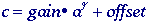
where
 is the gamma of the recording medium.
For a truly linear recording system we must have
= 1 and offset = 0. Unfortunately, the
offset is almost never zero and thus we must compensate for this if the
intention is to extract intensity measurements. Compensation techniques
are discussed in Section 10.1. is the gamma of the recording medium.
For a truly linear recording system we must have
= 1 and offset = 0. Unfortunately, the
offset is almost never zero and thus we must compensate for this if the
intention is to extract intensity measurements. Compensation techniques
are discussed in Section 10.1.
Typical
values of
that may be encountered are listed in Table 8.
Modern cameras often have the ability to switch electronically between
various values of
.
|
Sensor
|
Surface
|
|
Possible
advantages
|
|
CCD chip
|
Silicon
|
1.0
|
Linear
|
|
Vidicon Tube
|
Sb2S3
|
0.6
|
Compresses
dynamic range -> high contrast scenes
|
|
Film
|
Silver
halide
|
<
1.0
|
Compresses
dynamic range -> high contrast scenes
|
|
Film
|
Silver
halide
|
>
1.0
|
Expands dynamic range ->
low contrast scenes
|
Table 8:
Comparison of
of
various sensors
There
are two ways to describe the sensitivity of a camera. First, we can
determine the minimum number of detectable photoelectrons. This can be
termed the absolute sensitivity. Second, we can describe the
number of photoelectrons necessary to change from one digital brightness
level to the next, that is, to change one analog-to-digital unit
(ADU). This can be termed the relative sensitivity.
To determine the absolute
sensitivity we need a characterization of the camera in terms of its
noise. If the total noise has a
 of,
say, 100 photoelectrons, then to ensure detectability of a signal we
could then say that, at the 3
level, the minimum detectable signal (or absolute sensitivity) would be
300 photoelectrons. If all the noise sources listed in Section 6, with
the exception of photon noise, can be reduced to negligible levels, this
means that an absolute sensitivity of less than 10 photoelectrons is
achievable with modern technology of,
say, 100 photoelectrons, then to ensure detectability of a signal we
could then say that, at the 3
level, the minimum detectable signal (or absolute sensitivity) would be
300 photoelectrons. If all the noise sources listed in Section 6, with
the exception of photon noise, can be reduced to negligible levels, this
means that an absolute sensitivity of less than 10 photoelectrons is
achievable with modern technology
The definition of relative
sensitivity, S, given above when coupled to the linear case, eq.
with
=
1, leads immediately to the result:
The
measurement of the sensitivity or gain can be performed in
two distinct ways.
*
If, following eq. , the input signal a can be precisely
controlled by either "shutter" time or intensity (through
neutral density filters), then the gain can be estimated by estimating
the slope of the resulting straight-line curve. To translate this into
the desired units, however, a standard source must be used that emits a
known number of photons onto the camera sensor and the quantum
efficiency (
 ) of the sensor must be known. The quantum
efficiency refers to how many photoelectrons are produced--on the
average--per photon at a given wavelength. In general 0 <=
( ) of the sensor must be known. The quantum
efficiency refers to how many photoelectrons are produced--on the
average--per photon at a given wavelength. In general 0 <=
(
 ) <= 1. ) <= 1.
*
If, however, the limiting effect of the camera is only the photon
(Poisson) noise (see Section 6.1), then an easy-to-implement,
alternative technique is available to determine the sensitivity. Using
equations , , and and after compensating for the offset (see
Section 10.1), the sensitivity measured from an image c is
given by:
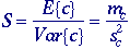
where
mc and sc are defined in equations
and .
Measured
data for five modern (1995) CCD camera configurations are given in Table
9.
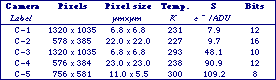
Table
9:
Sensitivity measurements. Note that a more sensitive camera has a lower
value of S.
The
extraordinary sensitivity of modern CCD cameras is clear from these
data. In a scientific-grade CCD camera (C-1), only 8 photoelectrons
(approximately 16 photons) separate two gray levels in the digital
representation of the image. For a considerably less expensive video
camera (C-5), only about 256 photoelectrons (approximately 512 photons)
separate two gray levels.

As
described in Section 6, in modern camera systems the noise is frequently
limited by:
*
amplifier noise in the case of color cameras;
*
thermal noise which, itself, is limited by the chip temperature K and
the exposure time T, and/or;
*
photon noise which is limited by the photon production rate
 and the exposure time T. and the exposure time T.
Using cooling techniques based
upon Peltier cooling elements it is straightforward to achieve chip
temperatures of 230 to 250 K. This leads to low thermal electron
production rates. As a measure of the thermal noise, we can look at the
number of seconds necessary to produce a sufficient number of thermal
electrons to go from one brightness level to the next, an ADU, in the
absence of photoelectrons. This last condition--the absence of
photoelectrons--is the reason for the name dark current.
Measured data for the five cameras described above are given in Table
10.
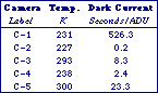
Table 10:
Thermal noise characteristics
The
video camera (C-5) has on-chip dark current suppression. (See
Section 6.2.) Operating at room temperature this camera requires more
than 20 seconds to produce one ADU change due to thermal noise. This
means at the conventional video frame and integration rates of 25 to 30
images per second (see Table 3), the thermal noise is negligible.
From eq. we see that it should
be possible to increase the SNR by increasing the integration
time of our image and thus "capturing" more photons. The
pixels in CCD cameras have, however, a finite well capacity. This finite
capacity, C, means that the maximum SNR for a CCD camera
per pixel is given by:
Capacity-limited
photon noise -

Theoretical
as well as measured data for the five cameras described above are given
in Table 11.
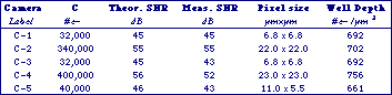
Table 11:
Photon noise characteristics
Note
that for certain cameras, the measured SNR achieves the
theoretical, maximum indicating that the SNR is, indeed, photon
and well capacity limited. Further, the curves of SNR versus T
(integration time) are consistent with equations and . (Data not shown.)
It can also be seen that, as a consequence of CCD technology, the
"depth" of a CCD pixel well is constant at about 0.7 ke-
/ um2.
Virtually all imaging systems
produce shading. By this we mean that if the physical input image a(x,y)
= constant, then the digital version of the image will not be
constant. The source of the shading might be outside the camera such as
in the scene illumination or the result of the camera itself where a gain
and offset might vary from pixel to pixel. The model for shading
is given by:

where
a[m,n] is the digital image that would have been
recorded if there were no shading in the image, that is, a[m,n]
= constant. Techniques for reducing or removing the effects of
shading are discussed in Section 10.1.
While
the pixels shown in Figure 1 appear to be square and to
"cover" the continuous image, it is important to know the
geometry for a given camera/digitizer system. In Figure 18 we define
possible parameters associated with a camera and digitizer and the
effect they have upon the pixel.
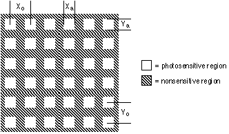
Figure 18:
Pixel form parameters
The
parameters Xo and Yo are the spacing
between the pixel centers and represent the sampling distances from
equation . The parameters Xa and Ya
are the dimensions of that portion of the camera's surface that is
sensitive to light. As mentioned in Section 2.3, different video
digitizers (frame grabbers) can have different values for Xo
while they have a common value for Yo.
As mentioned in Section 5,
square sampling implies that Xo = Yo
or alternatively Xo / Yo = 1. It is
not uncommon, however, to find frame grabbers where Xo
/ Yo = 1.1 or Xo / Yo
= 4/3. (This latter format matches the format of commercial television.
See Table 3) The risk associated with non-square pixels is that
isotropic objects scanned with non-square pixels might appear isotropic
on a camera-compatible monitor but analysis of the objects (such as
length-to-width ratio) will yield non-isotropic results. This is
illustrated in Figure 19.
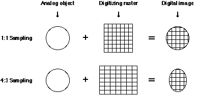
Figure 19:
Effect of non-square pixels
The
ratio Xo / Yo can be determined for
any specific camera/digitizer system by using a calibration test chart
with known distances in the horizontal and vertical direction. These are
straightforward to make with modern laser printers. The test chart can
then be scanned and the sampling distances Xo and Yo
determined.
In modern CCD cameras it is
possible that a portion of the camera surface is not sensitive to light
and is instead used for the CCD electronics or to prevent blooming.
Blooming occurs when a CCD well is filled (see Table 11) and additional
photoelectrons spill over into adjacent CCD wells. Anti-blooming regions
between the active CCD sites can be used to prevent this. This means, of
course, that a fraction of the incoming photons are lost as they strike
the non-sensitive portion of the CCD chip. The fraction of the surface
that is sensitive to light is termed the fill factor and
is given by:

The
larger the fill factor the more light will be captured by
the chip up to the maximum of 100%. This helps improve the SNR.
As a tradeoff, however, larger values of the fill factor mean more
spatial smoothing due to the aperture effect described in Section 5.1.1.
This is illustrated in Figure 16.
Sensors, such as those found in
cameras and film, are not equally sensitive to all wavelengths of light.
The spectral sensitivity for the CCD sensor is given in Figure 20.
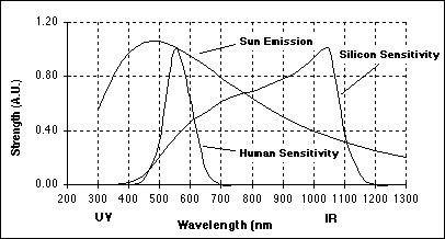
Figure
20:
Spectral characteristics of silicon, the sun, and the human visual
system. UV = ultraviolet and IR = infra-red.
The
high sensitivity of silicon in the infra-red means that, for
applications where a CCD (or other silicon-based) camera is to be used
as a source of images for digital image processing and analysis,
consideration should be given to using an IR blocking filter. This
filter blocks wavelengths above 750 nm. and thus prevents
"fogging" of the image from the longer wavelengths found in
sunlight. Alternatively, a CCD-based camera can make an excellent sensor
for the near infrared wavelength range of 750 nm to 1000 nm.
The
length of time that an image is exposed--that photons are collected--may
be varied in some cameras or may vary on the basis of video formats (see
Table 3). For reasons that have to do with the parameters of
photography, this exposure time is usually termed shutter speed
although integration time would be a more appropriate description.
Values of the shutter speed as
low as 500 ns are available with commercially available CCD video
cameras although the more conventional speeds for video are 33.37 ms (NTSC)
and 40.0 ms (PAL, SECAM). Values as high as 30 s may also be achieved
with certain video cameras although this means sacrificing a continuous
stream of video images that contain signal in favor of a single
integrated image amongst a stream of otherwise empty images. Subsequent
digitizing hardware must be capable of handling this situation.
Again values as low as 500 ns
are possible and, with cooling techniques based on Peltier-cooling or
liquid nitrogen cooling, integration times in excess of one hour are
readily achieved.
The rate at which data is read
from the sensor chip is termed the readout rate. The
readout rate for standard video cameras depends on the parameters of the
frame grabber as well as the camera. For standard video, see Section
2.3, the readout rate is given by:
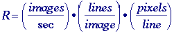
While
the appropriate unit for describing the readout rate should be pixels
/ second, the term z is frequently found in the literature
and in camera specifications; we shall therefore use the latter unit.
For a video camera with square pixels (see Section 7.5), this means:
|
Format
|
lines
/ sec
|
pixels
/ line
|
R
(Mz.)
|
|
NTSC
|
15,750
|
(4/3)*525
|
~11.0
|
|
PAL / SECAM
|
15,625
|
(4/3)*625
|
~13.0
|
Table 12:
Video camera readout rates
Note
that the values in Table 12 are approximate. Exact values for
square-pixel systems require exact knowledge of the way the video
digitizer (frame grabber) samples each video line.
The
readout rates used in video cameras frequently means that the electronic
noise described in Section 6.3 occurs in the region of the noise
spectrum (eq. ) described by
 >
max
where the noise power increases with increasing frequency. Readout noise
can thus be significant in video cameras. >
max
where the noise power increases with increasing frequency. Readout noise
can thus be significant in video cameras.
Scientific
cameras frequently use a slower readout rate in order to reduce the
readout noise. Typical values of readout rate for scientific cameras,
such as those described in Tables 9, 10, and 11, are 20 kz, 500 kz, and
1 Mz to 8 Mz.
|